ICs are of crucial importance for the EMC characteristics of electronic modules. They are a source of electromagnetic disturbances on the one hand but at the same time also help reduce these disturbances.
Measurement experience gained through volume and pin scans with near-field microprobes in the past shows that ICs of an identical design, i.e. function- and pin compatible ICs, can have very different EMC characteristics.
The IC test system based on near-field microprobes will enable developers to optimise EMC characteristics from the start of the design process to allow the low-cost development of ICs with good EMC characteristics.
INTRODUCTION
Measuring electromagnetic disturbance emissions is one part of the IC test system. According to international EMC standards for ICs, near-field microprobes are used which clearly exceed IEC standard requirements in terms of their measurement parameters such as resolution and frequency range. They thus allow the developers to measure electromagnetic
disturbance emissions on ICs and open DIEs and precisely localise
the respective field sources in the IC or DIE. IC redesign measures can thus be taken in the course of development which are derived from the measured results and ensuing known EMC measures. The aim is to minimise emissions from electromagnetic
disturbance field sources on the one hand and to pass the EMC conformity test within a reasonable time and at low cost on the other.Measuring system
MEASURING SYSTEM
Measuring spatial amplitude-frequency characteristics of electromagnetic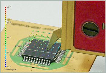 emissions requires an IC test system architecture with the following
components: near-field microprobes, a positioning system for the microprobes and a software to control the entire measuring sequence in the IC test system are needed in addition to a spectrum analyser.
Three types of near-field probes and a microprobe positioning system with at least four axes are necessary to completely detect EMC emissions from ICs.
The near-field probes comprise an E-field probe to measure the electric field and two H-field probes to measure the magnetic field. The two magnetic field probes differ in their plane of polarisation: The „h“ type H-field probe has a horizontal polarisation and the „v“ type H-field probe has a vertical polarisation. A set of microprobes thus always comprises E, Hh and Hv probes and the whole set is needed to detect all field components of EMC emissions.
The positioning system brings the microprobes in position and determines the spatial coordinates of the electromagnetic field. The directional pattern of the vertically polarised H-field probe has two zero values for physical reasons. The field components located in the plane of the vertical probe can only be detected by rotating the Hv-field probe. An IC test system with at least four axes, i.e. x, y, z and alpha axis, is thus used as a positioning system.
Figs. 1 and 10 show a schematic diagram of the IC test system setup for measurements based on the surface scan method according to IEC 61967. The dimensions of the near-field microprobes are around 0.15 mm. Due to their design, they allow the user to separately examine electrical and magnetic emissions on IC and DIE surfaces, bonding wires and pins. The probe‘s resolution and sensitivity require a precise positioning system which moves the probes from point to point within the measurement volume. The actual E or H-field probe is designed as a probe head at its tip. The complete probe is an active probe. The probe housing with the integrated measuring
amplifier is partially visible in Fig. 1. The active probe internally covers the frequency range from 16 kHz to 3 GHz. The IEC standard IEC 61967-3 range of 150 kHz to 1 GHz is completely covered and even exceeded by these probes.
The IC test system for near-field microprobes can incorporate all types of microprobes. These probes are moved from point to point in the measurement volume by the four-axis positioning system. The position of the probe tip is controlled via a digital microscope. The smallest increment is 5μm.
The IC test system, spectrum analyser and measuring sequence are controlled by a PC. The connected measuring and control devices are initialised after the control and operating software program of the IC test system have been started. The measuring ranges are then set for the spectrum analyser and positioning system via the graphic user interface. An instruction set is subsequently
started to implement the measuring algorithms. All measurements are carried out automatically. The measured data appear in real time in the visualisation area on the PC.
Fig. 2 shows the graphic user interface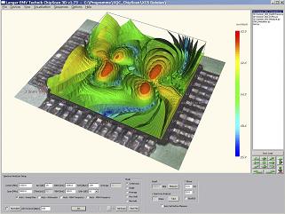 of the control and operating software of the IC test system. In addition to the menu bar, it comprises two device areas used to control the spectrum analyser and positioning system, a script window for measuring algorithms and a visualisation area for the 2D and 3D presentation of the measured results.
The visualisation area in Fig. 2 shows a three-dimensional surface scan. EMC emission measurements on IC provide large quantities of data that are compiled in six dimensions in a database. Not all six dimensions can be represented graphically at the same time, so that the representation is thus reduced to a feasible five dimensions. Dynamic images are needed for this purpose though these are not practicable in books and journals at present.
The near-field microprobes, operating software and device architecture of the IC test system allow the user to measure radiated EMC emissions and characterise the field distribution over the IC.
MEASUREMENTS ON A CALIBRATION STRIP LINE
The transmission factors of the microprobes are determined in the frequency range from 16 kHz to 3 GHz on the strip line. The measurement is based on the following parameters: the strip line has a width of 2 mm, a thickness of 35 μm and a termination of 50 ohm. The low end of the probe tip is adjusted to 25 μm over the strip line. The supply is implemented at 100 dBμV via the tracking generator of the spectrum analyser. Further measurements are carried out with these parameters to determine the transmission factors of the near-field microprobes. The characteristics of the 150μm near-field probes of types E, Hh and Hv can be found at http://www.langer-emv.de/produkte/IC-Nahfeldsonden.htm.
VOLUME SCAN OVER A 50 OHM STRIP LINE WITH A VERTICAL H-FIELD PROBE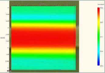
Fig. 3 shows a surface scan over the calibration strip line. The near-field microprobe with a vertical polarisation was used for this purpose. The measurement range is 6 mm x 6 mm symmetrically over the strip line. The vertically polarised probe measures high magnetic field strengths over the conductor run. High measurement levels are shown in red and low ones in blue. The probe‘s high selectivity becomes obvious in Fig. 3. The contours of the strip line are reproduced very well. Another field of application of this measuring method is the pin-selective measurement on all sides of an IC.
The automatic selective measurement of EMC emissions on all pins is quite fast.
Around 60 pins per minute can be measured. This method has been developed as a special EMC measurement procedure that enables
a universally valid assessment of all pins of a semiconductor in a short time.
Fig. 4 shows the measured results of the volume scan over the same strip line as a 3D presentation. The magnetic field lines are arranged in a circle around 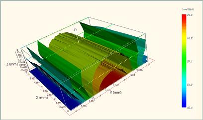 the conductor run. The measurement volume is 6 x 6 x 2 mm. All the results of the surface scan are confirmed and reproduced. The lowest area of the volume scan corresponds to the surface scan.
Fig. 4: Volume scan over the strip line with a vertical H-field microprobe
VOLUME SCAN OVER A 50 OHM STRIP LINE WITH A HORIZONTAL H-FIELD PROBE
Unlike the vertically polarised probe, the horizontal probe measures the centre of the calibrating strip line with a high selectivity. Intensive magnetic fields are located at the edges of the strip line, which is also the site of the respective local maximum values of the volume scan. The probe behaviour here is exactly opposite for the same measurement volume and at an identical probe resolution:
Vertical probe: Maximum over the conductor run Horizontal probe: Minimum over the conductor run Fig. 5: Volume scan over the strip line with a horizontal H-field microprobe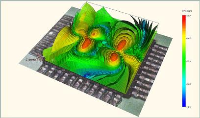
VOLUME SCAN OVER AN IC
Fig. 6 shows results measured during
the volume scan of an IC. The measurement volume is 11 x 11 x 1.6 mm over an IC with 44 pins. The field sources can be clearly and easily
localised. The field distribution on the surface indicates the inner IC structure. Locations of identical field strength are connected through ISO surfaces that are color-coded according
to their intensity (red: intensive disturbance emissions) in the spatial representation of the magnetic field.
Fig. 6: Volume scan over an IC: 3D presentation of the ISO field lines at a frequency peak of 50 MHz
VOLUME SCAN OVER AN OPEN DIE
Fig. 7 shows the measurement set-up for measuring EMC emissions on an open DIE.Fig. 7: High-resolution EMC scanner with digital microscope and horizontal near field microprobe on the open DIE
The positioning system performs the smallest probe movements in 5 μm increments. Larger increments are here necessary that are optimised in terms of measurement time and resolution.
The measurement volume is 8 x 8 x 2 mm. The magnetic field was measured in a total of 12,000 volume points. A comparison of the sizes of the DIE and measuring probe is shown in Fig. 8. Fig. 8: Comparison of size with a high-resolution EMC scanner: DIE and H field probe

Surface scans are available for all frequencies of the measuring interval, i.e. one complete surface scan per frequency point and volume plane, on completion of the measurement.
The field sources of the disturbances emissions can be localised through the surface scan‘s frequency value by selecting the peaks in the measured cumulative spectrum and setting the associated frequency in the evaluation software. Two ranges are visible at the clock frequency of 100 MHz in Fig. 9. The peak in the discrete frequency spectrum at 100 MHz is caused by two IC areas: cycle electronics in the DIE and the associated clock lines.
Fig. 9: Surface over DIE and bonding wires at a peak frequency of 50 MHz  Preliminary examinations on the PCB level are possible with spectrum analysers and near-field probes. In combination with an IC test system according to Fig. 10, the development
engineer can precisely localise EMC emissions as well as reproduce and document the measured results. Furthermore, various modifications aimed at reducing EMC emissions can be compared. The representation
of electric and magnetic fields as spatial amplitude-frequency characteristics is suitable for this purpose, particularly if IC housing forms such as BGA have to be used for layout reasons. The EMC conformity tests can thus be carried out within a reasonable time and at low cost without unforeseen surprises if IC tests are carried out gradually in the development process.
SUMMARY
Electromagnetic disturbance field sources are localised in ICs and open DIEs and their emissions are gradually minimised through high-resolution EMC scans in the development
process.
The electromagnetic disturbance emissions are measured with near-field microprobes, a spectrum analyser and a high-resolution positioning system that simultaneously determines
the spatial coordinates of the electromagnetic field.
EMC emission hot spots can be detected with the six-dimensional graphic representation of the measured results that is necessarily implemented in several planes as spatial amplitude- frequency characteristics.
The EMC test system can be used to characterise the electromagnetic emission behaviour of ICs. Function and pin-compatible ICs can be precisely classified in terms of their EMC characteristics for component applications.
The measurements on the calibration strip line with different near-field microprobes demonstrate that estimates can be made separately of the expected E-fields and H-fields. Measurements can be taken in the near-field range within a short time and with reproducible results. Structures of different fineness can be resolved and measured separately for the respective type of field by considering such parameters as distance (side/height), step width and present field strengths. Resolutions in the 100 μm range provide a detailed insight into the distribution and strength of fields and their potential disturbance emissions.
Consistencies between current and field measurements can be determined on the IC. The range of action and spectrum can be extracted in the result of these measurements. The visualisation area (Fig. 6 and Fig. 9) shows that differentiations can be made between individual PINs depending on the field orientation. This provides important IC development aids. Both E-fields and H-fields can be determined separately on small structures such as open DIEs with the near-field microprobes. The current- carrying paths of the IC can be tracked in the near field by the H-field measurement (see Fig. 6 and Fig. 10).
The time that is needed for this informative measuring method is around one hour and is thus irrelevant in practical laboratory work since the entire measurement including the complete
documentation of all measured results and measurement parameters takes place automatically.
This measuring method can also be used to provide IC developers with an efficient tool that allows them to assess the achieved qualification level of the semiconductor in the development process. If IC samples from different development stages are measured, the developer can measure and determine the effects of his changes to the IC in the near-field range. Conclusions can thus already be drawn during IC development and known EMC measures be implemented during the ongoing development process DETAILS ABOUT THE AUTHOR
Dr. E. Schubert is a development engineer for IC test systems at Langer
EMV-Technik GmbH